Using the Configurable Logic Cells (CLCs) and the Signal Routing (SR) port in the PIC18-Q71 family of microcontrollers (MCUs), it is possible to implement advanced self-test and input selection features.

How to Enhance the Performance of Microcontroller using CLCs and SR Port
The Configurable Logic Cells (CLCs) and the Signal Routing (SR) port are on-chip Core Independent Peripherals (CIPs). CIPs are specialized blocks of hardware that operate independently of the CPU core, enhancing the performance of the microcontroller (MCU) by expanding the capabilities of the MCU and/or minimizing overall power consumption. By using the CLC and SR Port CIPs in conjunction, users can implement a digital multiplexer for advanced self-test and input selection features in the microcontroller.
CLCs are internal blocks of programmable logic that can operate independently of the CPU. The CLCs are designed in various logical configurations, such as 4-input AND, SR Latch and, 1-input D Flip-flop with S and R.
The SR Port is a CIP that mimics an output I/O port but is only used internally. The SR Port can be used to interconnect signals from one CIP to another, implement hardware state machines and group CIP signals together into a single register.
Use Cases of SR Port and CLCs
One use case of the SR Port and CLCs is to implement a digital multiplexer. Multiplexers select one of N signals to output, usually labeled as N:1. For instance, a 2:1 multiplexer takes two signals and selects one. This software-defined implementation of a digital multiplexer is distinctly different than the Peripheral Pin Select (PPS) feature found on most modern PIC® microcontrollers.
PPS allows the I/O of a peripheral to be rerouted to a different pin on the microcontroller for design flexibility. However, PPS has a few limitations. For one, changing the PPS settings requires the software to modify the respective register value. But these registers may be locked by the application to prevent accidental changes, with an additional option of making them unlockable only once per device reset.
In contrast to PPS, the digital multiplexer using the SR port is a lot simpler to control. Unlike PPS, the SR Port can be read and written like a normal register, with no unlocking sequence required. And since the implementation is custom, the configuration of the bits within SR Port are controllable by the developer. At runtime, the application can poll the status of the digital multiplexer by simply reading the value of the bit in the SR Port.
This implementation may be used in a few ways. For instance, if there was an application that had four Universal Asynchronous Receiver/Transmitter (UART) inputs to receive from, but only one UART receiver, the inputs could be multiplexed through the SR port to select which input signal to decode. Another use case could be to multiplex multiple internal output signals onto a single I/O pin.
The use case that this blog post will focus on is as part of a self-test feature, which could contribute to Functional Safety (FuSa) in the design. In this setup, the digital multiplexer selects between an internal test pattern and the actual signal. On startup, the microcontroller selects the test pattern input and verifies the receiver/decoder/timer functions as expected.
As a hypothetical example, consider an application where the pulse width of a signal is being measured using a Universal Timer (UTMR). The objective of the UTMR in this application is to measure the on time of the pulse and to ensure the pulse width is never above a certain length.
One input of the digital multiplexer is connected to the desired I/O pin, while the other is connected to the internal test pattern source, such as standalone Pulse Width Modulator (PWM) or another one of the bits from the SR Port for a custom, bit-banged solution.
On startup, the internal pattern source is selected and the test signal is generated. If the UTMR is working properly, the known pulse width of the input should be capturable by the UTMR. Once the application validates the UTMR is operating as expected, the multiplexer can transparently switch over to the external I/O pin without interruption.
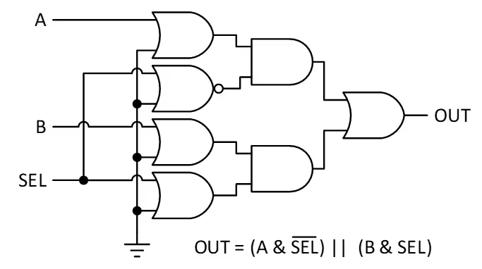
To implement a simple 2:1 multiplexer, the logic function to implement a digital multiplexer is the following:
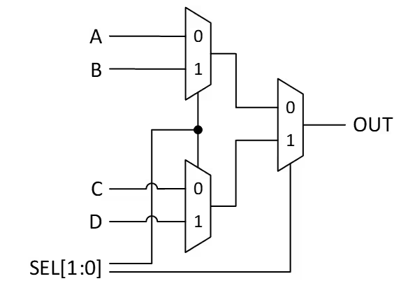
A larger 4:1 multiplexer is substantially more complicated. CLCs have four inputs, and there is a total of six signals—four inputs and two selections bits—required in this configuration. But the 4:1 multiplexer can still be implemented with three 2:1 multiplexers (three cells), as shown below.
The CLC and SR Port are powerful CIPs that allow users to develop custom logic circuits inside of the microcontroller. One application of these peripherals is to make a digital logic multiplexer to select internal signals or as part of an advanced self-test routine. CLCs and an SR Port are available on the PIC18-Q71 family of microcontrollers. More information about FuSa on 8-bit microcontrollers can be found on our web page.
Robert Perkel, Jun 6, 2023
Tags/Keywords: Automotive and Transportation
Commentaires